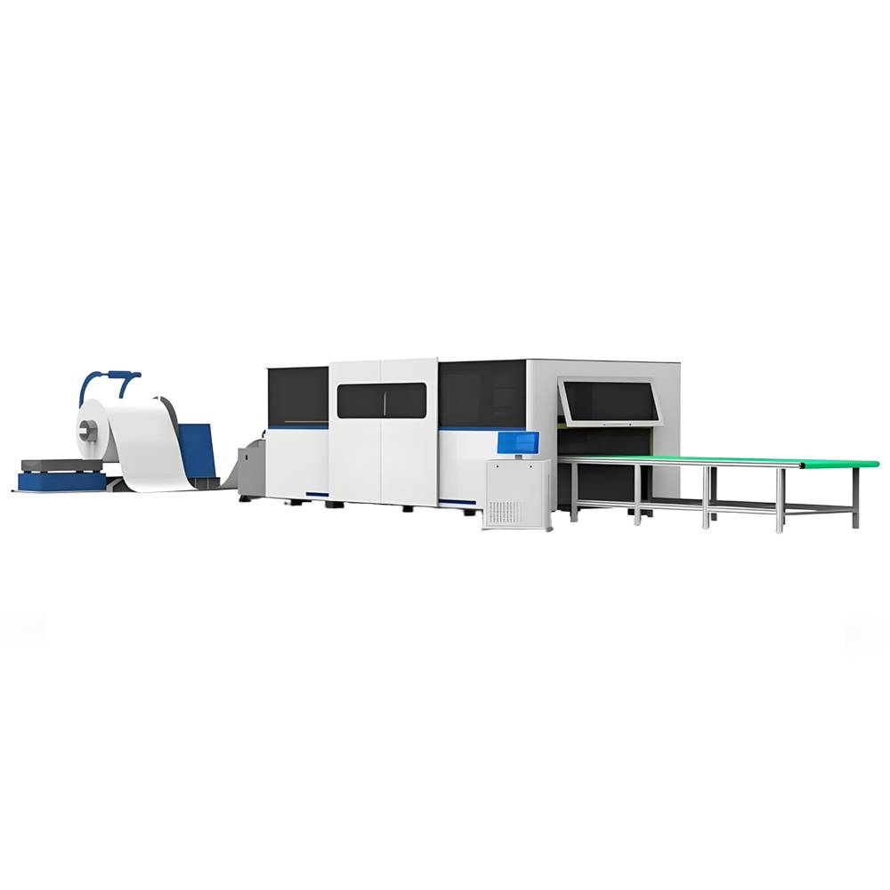
Laser 3D printer, an “all-round player” in the industry
22 Sep
Recently, researchers at the University of Missouri in the United States have developed a method that can make complex devices with a variety of materials, including plastics, metals and semiconductors, with just one machine. The study, recently published in Nature Communications, outlines a new 3D printing and laser process for making multi-material, multi-layer sensors, circuit boards, and even textiles with electronic components. The research, called the “free-form multi-material assembly process,” is expected to revolutionize the manufacturing process of new products. By printing sensors embedded in structures, the machine can create devices that can sense environmental conditions, including temperature and pressure. For other researchers, this may mean having a natural-looking object, such as a rock or shell, that can measure the flow of seawater. For the public, this application lays the technical foundation for future wearable devices that monitor blood pressure and other vital signs.
Specifically, other technologies fall short in the versatility of materials and how to precisely place smaller parts into larger 3D structures. The research team’s approach solves these problems using special techniques. Team members built a machine with three different nozzles: one nozzle adds ink-like material, another uses a laser to carve shapes and materials, and a third nozzle adds additional functional materials to enhance the product’s functionality. First, the basic structure is made with ordinary 3D printing filaments (such as polycarbonate, a transparent thermoplastic). Then, a laser is used to convert certain parts into a special material called laser-induced graphene and place it exactly where it is needed. Finally, more materials are added to enhance the functionality of the final product. “This work was supported by the National Science Foundation (NSF) Advanced Manufacturing Program, and the NSF I-CorpsTM program provided funding to explore commercialization. The I-Corps program is helping the research team identify market interests and needs,” said Jian “Javen” Lin, associate professor of mechanical and aerospace engineering at the university. “At this time, we think other researchers will be interested in it, but we believe it will ultimately benefit companies. It will reduce the time it takes to prototype a device, allowing companies to make prototypes in-house.” This is the first time this process has been used, and it opens up new possibilities, said Bujingda Zheng, the study’s first author and a doctoral student in mechanical engineering at the University of Missouri. “I’m very excited about this design. One of the main benefits is that innovators can focus on new product design without worrying about how to make prototypes. This opens up the possibility of entirely new markets.” Lin said it will have a wide impact on wearable sensors, customizable robots, medical devices, and more. Currently, manufacturing multi-layer structures such as printed circuit boards is a cumbersome process involving multiple steps and multiple materials. These processes are costly, time-consuming, and produce waste that is harmful to the environment. The new technology is not only better for the earth, but also inspired by systems in nature. For example, electric eels have skeletons and muscles that enable them to move, Zheng said. They also have specialized cells that can deliver up to 500 volts to deter predators. These biological observations have inspired researchers to develop new ways to make three-dimensional structures with versatile applications, but other emerging methods have limitations.


 0531-87978823
 +86 16653132325
 sales01@raytu.com
 Contact us